


Product Description
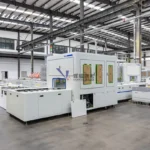
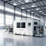
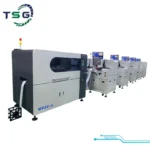
The Right Wafer Die Bonder is a high-precision, high-efficiency automatic equipment independently developed by Right (Zhengshi) Automation, specialized in wafer die bonding process, which is a core device in the semiconductor packaging and advanced manufacturing production line. As a key equipment supporting 3D IC integration, MEMS packaging, power device manufacturing and other fields, it integrates advanced visual positioning, high vacuum system, precise temperature control and intelligent control technology, realizing fully automatic, high-precision bonding of various wafer dies, and is widely used in semiconductor, automotive electronics, optoelectronics, MEMS and other high-tech fields, helping enterprises improve production efficiency, reduce labor costs and enhance product competitiveness[2].
With ultra-high bonding precision of ±0.005mm and alignment precision of ±0.5μm, the Right Wafer Die Bonder effectively solves the pain points of die offset, uneven bonding force, high void rate and low consistency in traditional wafer die bonding processes. It supports wafer sizes from 2 to 12 inches and die sizes from 0.15×0.15mm to 30×30mm, compatible with silicon wafers, sapphire wafers and compound semiconductor wafers, meeting diverse production needs of semiconductor packaging industry. The working speed is adjustable from 1800 to 3800 pcs/hour, and the maximum speed can reach 4200 pcs/hour for standard dies, supporting 24/7 continuous operation without manual intervention, which can efficiently meet the needs of medium and large-scale mass production.
Equipped with dual HD CCD visual positioning system, AI visual compensation technology and high-precision optical alignment system, the equipment can automatically identify wafer die polarity, wafer Mark points and substrate Mark points, realize real-time precise positioning and automatic alignment, greatly reduce human error and ensure the consistency of bonding quality. It is equipped with a high vacuum system with ultimate vacuum of 10 Pa, which can effectively remove gas molecules at the bonding interface, reduce the bonding void rate to less than 1%, and improve the reliability and service life of products. The multi-zone independent PID temperature control system with temperature range of 25–450ºC and temperature uniformity of ±0.5ºC can adapt to different bonding processes such as epoxy glue bonding, conductive adhesive bonding and eutectic bonding, and support both temporary and permanent bonding processes to meet diverse process requirements.
The equipment adopts PLC + 12-inch industrial touch screen control, with a simple and user-friendly operation interface, supporting one-click process parameter recall, multi-language switching, and easy learning without professional training. It can be seamlessly connected to MES/ERP systems, realizing real-time upload of production data, batch traceability, and remote monitoring, which complies with the quality control standards of modern semiconductor manufacturing industry. With a compact structure, stable performance, and low energy consumption, it is suitable for factory workshops of all sizes, and is the core equipment for semiconductor manufacturing enterprises to realize automatic upgrading of the wafer die bonding process and improve production efficiency and product quality. Compared with imported equipment, it has higher cost performance and faster after-sales response, breaking the monopoly of overseas brands in the middle and high-end wafer die bonding equipment market.
| Machine Dimension |
1800×1700×2200mm (Compact Design, Space-Saving, Suitable for Various Clean Workshop Sizes)
|
|
Weight |
750kg |
|
Origin |
China |
Dispensing Technology |
Precision screw |
|
PowerSupply |
AC 220V, 50/60 Hz, 3.5KW |
|
Trademark |
Right |

Product Selling Points
Ultra-High Precision Bonding: Bonding precision ±0.005mm, alignment precision ±0.5μm, angle precision ±0.008°, dual CCD visual positioning with AI compensation, ensuring no die offset, uniform bonding force, and high product qualification rate (≥99.9%), perfectly matching the high-precision requirements of semiconductor wafer die bonding[4].
High Efficiency & Stable Operation: Working speed 1800–3800 pcs/hour (adjustable), max 4200 pcs/hour, support 24/7 continuous operation, greatly improving production efficiency and reducing labor costs, adapting to medium and large-scale mass production of semiconductor packaging.
Wide Compatibility for Wafers & Dies: Support wafer sizes 2–12 inches (50–300mm) and die sizes 0.15×0.15mm ~ 30×30mm, compatible with silicon wafers, sapphire wafers, compound semiconductor wafers, and various dies (semiconductor, MEMS, LED, power device), meeting diverse production needs.
Advanced Vacuum & Temperature Control: High vacuum system (ultimate vacuum 10 Pa) reduces bonding void rate to <1%; multi-zone PID temperature control (25–450ºC, uniformity ±0.5ºC), adapting to temporary and permanent bonding processes, ensuring stable bonding quality.
Reviews
Clear filtersThere are no reviews yet.